Thick Film Substrates & Packages (Screen Printing)
Features

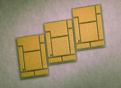
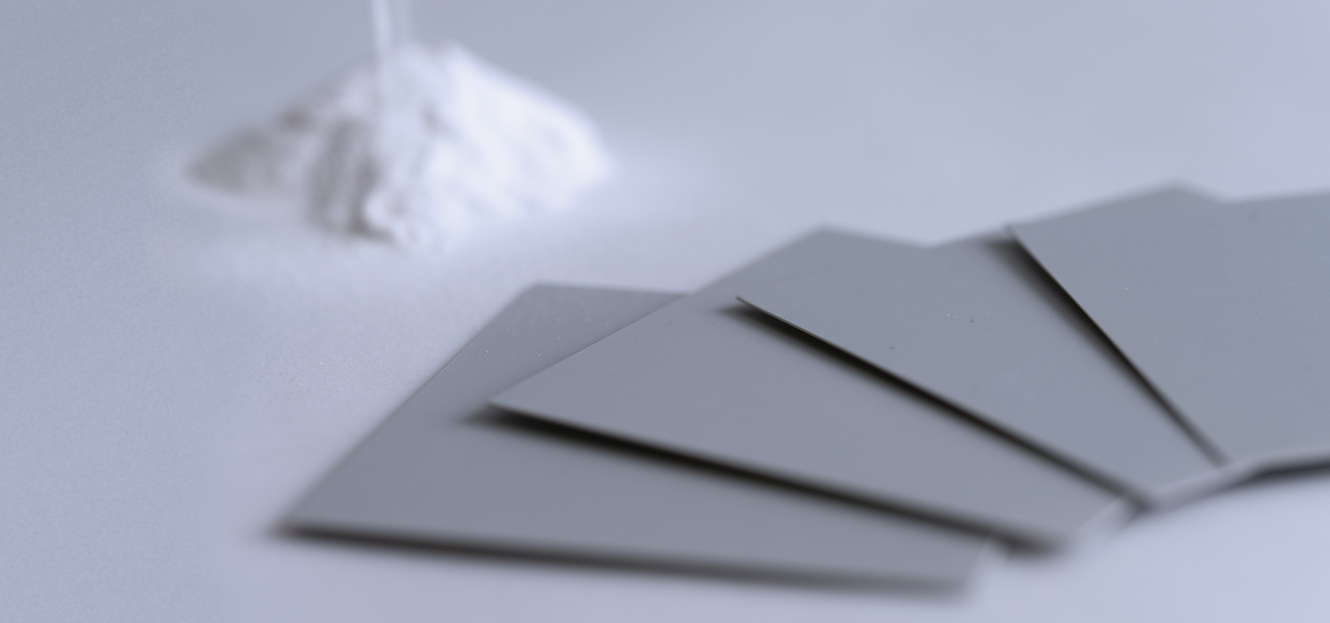
Thick film printed and high temperature sintered substrates using excellent thermal conductivity materials, Alumina and Aluminum Nitride (AlN).
Electrode formed ceramic substrates can be miniatuarized and multifunctional.
VIA structure can connect between top and bottom surfaces.
Structure sample (cross-section)

Applications
Sensor Packages, surface-mount packages, MEMS packages, Optical communication packages, LED packages, etc
Standard specification for Thick Film Metallization (screen printing)
| Item | Material | |||
| Substrate | Al2O3(92%) | AlN | ||
| Structure | Single layer |
|
Single layer |
|
|---|---|---|---|---|
| Metallized VIA | Mo / W / Cu / Ag | Mo / W | W / Cu | W |
| Inner layer | - | W | - | W |
| Surface layer | W / Cu / Ag | W / Cu / Ag | Cu (Plating specification can be applied) | W / Cu |
| Plating | NiB / NiP-Au / NiP-Pd-Au(Electroless plating) / Ni-Au(Electrolytic plating) | |||
Substrate characteristics
| Item | Unit | Material | ||||
|---|---|---|---|---|---|---|
| Al2O3(92%) | AlN | |||||
| Color | - | White | Brown | Gray | ||
| Bulk density | g/㎤ | 3.60 | 3.80 | 3.30 | ||
| Mechanical characteristics | Bending strength | MPa | 350 | 350 | 350 | |
| Thermal characteristics | Coefficient of thermal expansion | ppm/℃ | 7.0 | 7.3 | 4.6 | |
| Thermal conductivity | W/(m・K) | 16 | 15 | 170 | ||
| Electrical characteristics | Dielectric constant | 1GHz | - | 9.0 | 9.1 | 8.5 |
| Volume resistivity | 100Vdc | Ω・㎝ | >1014 | >1014 | >1014 | |
| Breakdown strength | ㎸/mm | >15 | >15 | >15 | ||

